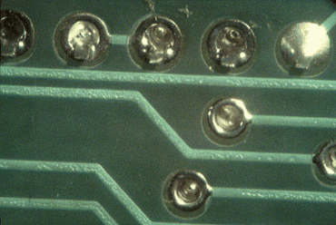
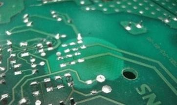
Solder Paste Inspection, abbreviated as SPI, is a specialized process that evaluates/inspects solder paste deposit quality on PCBs. It ensures the correct deposition of solder paste on the board without faults. In most of the cases, the reason behind the improper functioning of the PCB is due to improper solder paste printing. Solder paste inspection is therefore an essential technique that ensures costs are kept as low as possible by detecting faults in the solder printing stage of the production line. Solder paste deposition during a printing process is an indispensable task to attach the components to a circuit board for maintaining a proper electrical connection.
WORLD’s Surface Mount Technology (SMT) inspection process utilizes both Automated Optical Inspection (AOI) and X-ray to visually scan the surface of the board using high-definition (HD) cameras and several light sources. These systems use the captured image and compare it with the ideal/conventional board image which is already saved in the system. A comparison is then made between the captured image and the ideal image to detect and highlight any defects or suspected areas.
World electronics uses AOI (Automated Optical Inspection) and X-ray for solder paste inspection and defects analysis on every PCB because we believe in quality.
Automated Optical Inspection (AOI)
AOI machine tests and evaluates PCBs for faults like presence or absence, component placement defects, dimensional defects, and surface defects. With the advancement of electronic contract manufacturing and circuit complexity, it has become unfeasible to manually perform SMT inspection. Thus, AOI plays an important role in boards after PCB assembly. The machine has the capability of detecting errors in the early stage of the manufacturing process to assure the PCB quality before moving to the next manufacturing step.
WORLD electronics has one AOI machine, made by Yestech. It uses a camera and light to scan the surface of the board for defects such as backward parts (polarity), shorts, opens, missing components, and incorrect parts, among others. The machine uses already installed SW and templates and compares them to the board it is scanning. If the scanned board doesn’t match with the template (sometimes by a certain percentage), the part and board will be flagged, and the defects will be highlighted.
This technique inspects the PCB by using captured images to check:
- Are components missing?
- Are components placed in the correct position?
- Are there defects?
- Are we able to validate the quality of the manufacturing process?
The AOI machine can inspect all size components such as 01005, 0201, and 0402s and packages like CSPs, BGAs, LGAs, PoPs, and QFNs. Initially, AOI machines were designed for 2D measurements/analysis (detection along X and Y coordinates only). With the addition of 3D systems, the measurement along Z coordinate has also become possible. At WORLD, we use a 3D AOI machine for measurement along all the axis. The ultimate aim of an AOI machine is to detect errors in the production line and immediately informing the same to AOI programmers (also known as feedback). Feedback to the AOI programmers is both helpful and necessary so that time could be saved during SMT inspection.
AOI Programmers
The Automated Optical Inspection machine runs on a dedicated program, developed by AOI programmers. The following are the situations under which feedback is generated:
- Part descriptions are missing
- The search area needs to be modified
- Part markings need to be corrected, added, or deleted
SMT Inspection/Bare PCB Inspection via WORLD’s AOI Machine
WORLD’s 3D AOI machine tests PCB assembly for the following aspects:
- Area defects
- Component offset
- Component presence or absence
- Component polarity
- Component skew
- Excessive solder joints
- Height defects
- Flipped component
- Insufficient paste around leads
- Insufficient solder joints
- Lifted leads
- No population tests
- Paste registration
- Severely damaged components
- Volume defects
- Tombstoning
- Wrong part
- Solder bridging
- Existence of foreign material on the board
X-Ray Inspection System/Automated X-ray Inspection (AXI)
A PCB X-ray inspection system, also known as Automated X-ray Inspection (AXI), uses X-ray radiation instead of visible light to identify hidden PCB defects such as:
- Solder bridging under a BGA
- Tilted BGA and BGA voiding
- BGA missing balls
- BGA bad wetting
- Solder voids in pad areas
- Thermal defects
- QFN part defects
The above-mentioned defects can’t be seen during the inspection by standard cameras or by the naked eye. X-ray inspection is a commonly used technique that can detect manufacturing defects. The X-ray inspection machine can inspect the PCB from any angle.
WORLD electronics currently uses a 2D X-ray inspection system and are planning to upgrade it to a 3D AXI in the near future.
Structure/Principle of Operation for X-ray Machine
An inspection device based on X-rays consists of a chamber with a small gap where it is possible to insert and remove the PCB. The X-ray source is usually located at the bottom of the chamber. Within the chamber, a digital detector (phosphor screens) is positioned directly above the X-ray source. Using an edge conveyor belt, the PCB that needs to be examined enters the chamber and is located between the source and the detector. The backside of the PCB is exposed to the X-ray so that the X-ray can pass through the components.
While AOI produces full color images of the object surface, X-ray machine transmits X-rays through the objects and records grey scale images of the shadows. The image processing software then processes the image. It then detects the location and size/shape of expected features (for process optimization) along with the presence/absence of foreign objects or features (for anomaly detection).
Inside the component, the different molecular densities attenuate the X-rays by different amounts, resulting in the creation of light and dark areas in detective media. Consequently, we can easily identify cracks, i.e. the attenuation level of the dense part of the solder ball is heavy compared to the attenuation level of the crack or air. The crack tends to be dark due to varying attenuation levels, and the dense portion of the solder ball appears as a light in the image.
Conclusion of AOI and X-ray SPI
Solder paste inspection is a vital part in a PCB production line. It is crucial to identify solder paste defects in the early production cycle, otherwise, it can cost you both time and money. WORLD electronics’ AOI and X-ray machines use advanced SMT inspection techniques to offer quality and defects-free PCBs to our customers.
For more on WORLD’s capabilities visit our services page and follow us on LinkedIn.
Related Articles