Different types of testing and inspection processes are carried out during PCB manufacturing to ensure its quality. Methods such as PCB burn-in testing check for potential defects that can hamper the PCB functionality and remove them prior to shipping or installation. There are several inspection and testing techniques available in the market. WORLD electronics offers a complete set of formidable tests that detect the root cause of faults and prevent wasted time, effort, and resources. Two such inspection techniques, AOI and X-ray inspection, have been discussed previously in our “PCB Solder Paste Inspection” article.
It is critical for our customers to locate product flaws before their circuit boards make it into the field. WORLD offers exhaustive and thorough testing processes, including different methods: burn-in testing, in-circuit testing, and functional testing. Our three temperature chambers allow temperature cycling so that our clients can rest assured of the quality of their finished product.
PCB Burn-in Testing
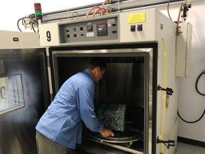
Burn-in is the testing of a PCB to detect early failures and establish load capacity. This is often done by running a power supply and firmware through the electronics for 12 to 48 hours. This testing process is intended to outline possible defects by running products at elevated voltage levels, outside standard temperature ranges, and under power cycling conditions.
The burn-in process enables the detection of components that will fail not only because of a specific physical defect but also because of a more general failure that occurred during assembly. The motive is to identify and replace failed components during the initial phase of the burn-in testing.
PCB Burn-in Testing at WORLD electronics
Burn-in testing first aims to ensure that the PCB design meets the specification for our clients’ various goals. The second is to cut out any part of the manufacturing process that may affect specific, individual components. WORLD is capable of testing throughout the manufacturing process or simply at the final stage.
After burn-in testing, we can better understand the load capacity of any given component and can say that the product meets our clients’ requirements. Having extensive experience with these processes, WORLD has refined its manufacturing process in a way that results in the failure of only a small number of assembled products, making manufacturing quicker and reliable. Our testing equipment has been carefully chosen to impose the most comprehensive, demanding, and reliable burn-in and temperature cycling processes among our competitors.
Our environmental chambers used for temperature cycling can become as cold as -84 degrees centigrade. At the other end of the spectrum, our low-mass Nichrome heating elements are used to reduce thermal lag and provide rapid response to instrument demanding up to 190 degrees C. It is better to identify those error-prone boards prior to sale rather than after delivery.
Click here to know more about PCB burn-in testing from our service portal.
PCB Functional Testing
A functional test is used as a final manufacturing step to validate that a PCB is free of defects. If untested, it may adversely affect the correct functioning of a device after integrating these boards into complete systems. In simple terms, a functional test verifies a PCB functionality and its behavior. PCB functional testing consists of a number of tests for qualifying board functionality, covering everything from checking for signal behavior to short circuits.
Apart from other tests that can be performed on any PCB, functional testing provides the most comprehensive view of a signal behavior. This goes beyond in-circuit testing, wherein individual components are examined after being soldered on a PCB. In contrast, PCB functional testing provides pass/fail determination on finished PCBs before shipping. At WOLRD electronics, we ensure that every tested PCB is fully compliant with IPC and ISO standards and guarantees a long working life.
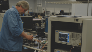
PCB Functional Testing at WORLD electronics
PCBs are tested within a system similar to which it was designed, which may involve the procurement of specific equipment and devices, to fully replicate their future working environment. As a full test service provider, WORLD electronics strives to provide comprehensive test strategies. As needed, WORLD can design new, custom test solutions to ensure our customers meet their specified test strategy. Functional test systems may include custom stand-alone systems, test firmware development, environmental stress screenings, or functional burn-in racks. Our highly skilled test technicians assemble and inspect based on IPC 610 and J-STD-001 standards. Our production facility is frequently audited and certified to these standards.
While several companies can conduct functional testing, WORLD’s dedication to providing full service means that we care for our clients at all stages of the production process, including testing. As a leading EMS provider, WORLD can comprehensively cater to your need for reliability and consistency with our in-house testing equipment. As such, we can thoroughly test our clients’ products using our equipment, equipment suggested by clients, or an amalgamation of both. A functional test may be as simple as a set of electronic measuring devices on a bench or as complex as a six-foot, rack-mounted, integrated testing system.
Click here to know more about PCB functional testing from our service portal.
WOLRD electronics’ extensive testing offers the following benefits:
- Reduced product development time
- Increased customer confidence
- 100% product quality and reliability
- A forecast life expectancy
- Reduced circuit board manufacturing costs
- Increased profitability
- Reduced after sales service
If desired, WORLD electronics will provide the most consistent, comprehensive, and precise testing of all its manufactured products. Reliable products are impossible to manufacture and place into the field without proven test strategies. Testing allows WORLD to reassure our clients that they receive the best possible product from us, every time.
For more on WORLD’s capabilities visit our services page and follow us on LinkedIn.
PCB Solder Paste Inspection Techniques