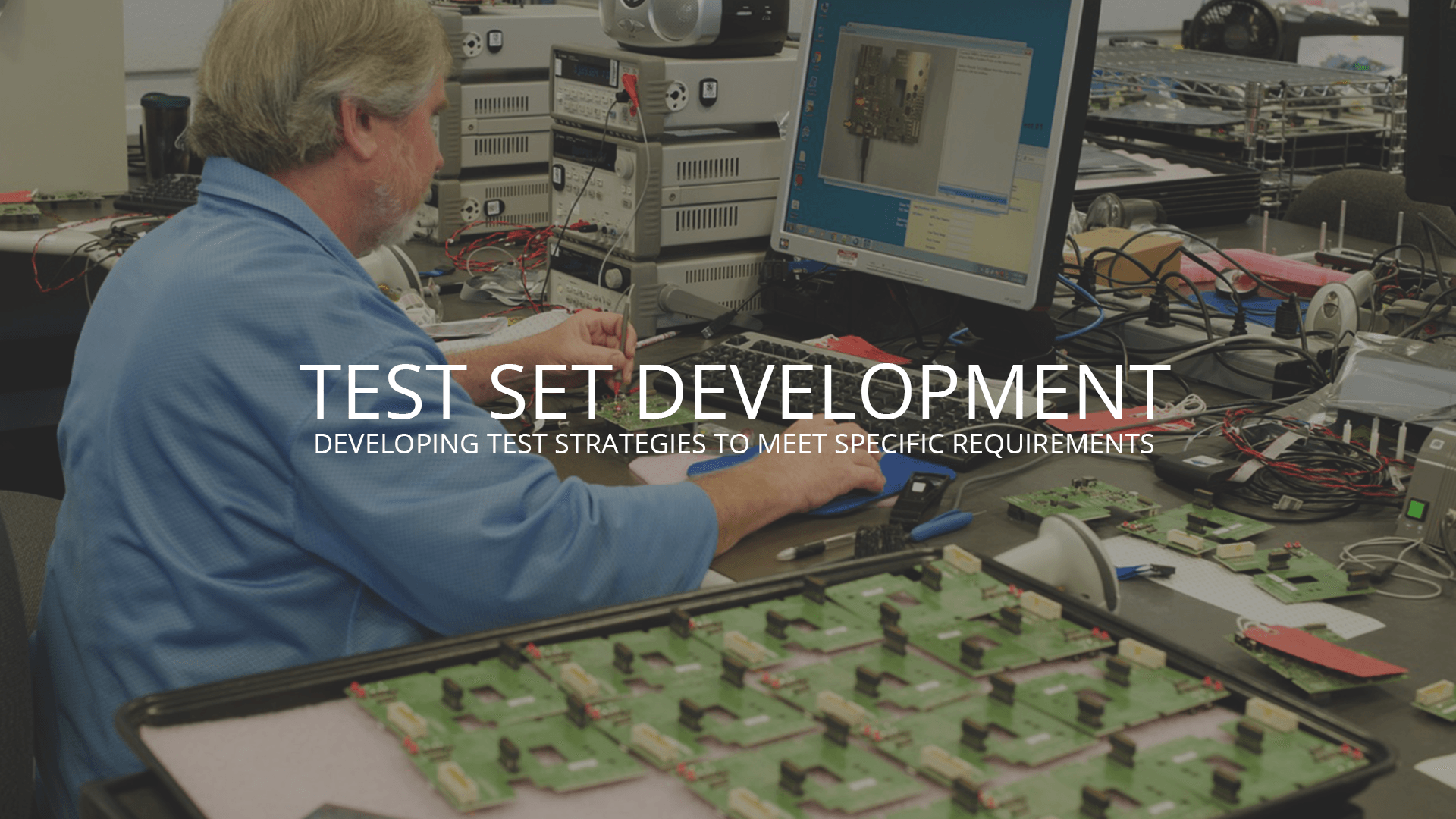
WORLD’s test engineering team supports our customer in two ways: by analyzing the existing test strategy and by providing economic solutions within the performance criteria. In the new product development (NPI) phase, WORLD’s test engineer’s partner with the customer to develop test strategies and hardware and software platforms to meet specific requirements.
In essence, test set development is relevant to every step of the design and manufacturing process. From the very beginning, designs must be conceived that are directly and easily testable, and this testing can take place throughout manufacture and assembly. Test set development refers to the creation of a testing plan, incorporating continual testing throughout the assembly, burn-in testing, and functional testing or In-Circuit test.
As a client, you can choose the complexity and comprehensiveness of the test set used on your product. Different methods of testing can cost more time and resources, and test for different outcomes; as such, it is possible to utilize as many methods as possible, or a bare minimum methods if cost and time frame are of concern.

In-circuit testing (ICT)
In-circuit testing is yet another of the many methods of testing undertaken by WORLD. PCB ICT is an example of testing wherein each individual PCB is checked for shorts, opens and functionality. ICT is one of the oldest forms of PCB testing and is most suitable for larger volume and stable designs. WORLD can perform a wide variety of tests on all its products, including ICT and functional testing, to maintain quality control. In the majority of production runs, WORLD utilizes every method of testing available in order to dramatically cut down on failures.
It is possible to manufacture PCBs without the use of ICT, although with larger volumes and stable designs and in the interest of quality control and the reduction of waste, it is recommended. That being said, other forms of testing like functional testing will always prevent the sale of unusable products.
Post-production testing
At the end of the production process, PCBs can be tested using a burn-in and/or temperature cycling process. These methods of testing are designed to push each board to the very limits of its function and prevents PCBs from failing after having been sold to the customer. Burn-in testing and temperature cycling ensure that the product received by the customer is practically guaranteed to have a long service life.
In addition to these methods, WORLD also utilizes functional testing: in other words, testing each finished product within the context it was manufactured. Functional testing is an ad hoc process that WORLD provides and is designed to meet the specific requirements of our clients. It is one of the most important steps during the complete manufacturing and testing process, and like other forms of testing is used to validate whether or not a particular product is suitable for shipping and free of defects. Functional testing involves ensuring that the final product functions as it was intended to do.
In order to fully replicate the product’s functional environment, it will be tested through use in an identical system to that of its intended use. This means testing it within a system that includes any device that communicates with the device and has an identical power supply to the one that the device will receive. The equipment necessary can either come from WORLD’s extensive test equipment collection or be provided by the customer. Additionally, WORLD has extensive National Instruments and Lab View development capabilities to meet any custom requirement.
As part of test set development, these concerns are balanced and a compromise can be reached as to how exactly the product is tested, and at which points of assembly. Each client has different needs, and WORLD is ready to address those needs with flexibility and attentiveness.