Different types of PCB cleaning methods are there used in the product of PCB assemblies. Three procedures are commonly utilized when it comes to PCB cleaning, each with its own set of benefits and drawbacks: manual cleaning, ultrasonic cleaning, and gas phase cleaning. The cleaning method you choose will be determined by the effectiveness, complexity, and density of the components on your PCB, the equipment you have access to, the cost and affordability, the number of boards to clean, the environmental impact, and the amount of time you have.
Manual Cleaning Method
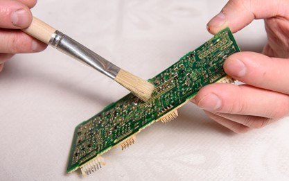
The hand cleaning method is one of the most prevalent methods of printed circuit board cleaning. Any contaminates or remaining solder substances are removed manually or physically, with an alcohol solution and a tiny brush. In addition to a brush, other equipment can be used to physically remove dirt from the board.
The manual cleaning method is popular since it is simple and inexpensive, as it does not require any equipment, and the supplies required are readily available. It is also thought to be a method with low toxicity to both humans and the environment. However, because this process lacks automation, it is more time consuming and may not be the optimal method for large batches of boards. The manual method is also limited in that you can only clean the sections of the board that are reachable with a brush or other cleaning equipment. As a result, this may not be the optimal option when it comes to cleaning fairly intricate or dense PCBs.
WORLD electronics hand cleans virtually all PCBs that it produces.
Ultrasonic Cleaning Method
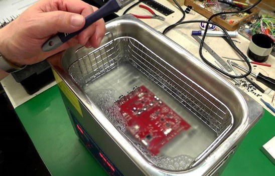
The ultrasonic cleaning process makes use of a machine designed specifically for cleaning PCBs. Similar to the manual technique, the board is first soaked in an ethyl alcohol solution to loosen dirt, contaminants, or extra soldering materials before being placed in the ultrasonic cleaner’s cleaning solution bath. The equipment emits high-frequency sound waves into the cleaning solution’s liquid bath, causing billions of tiny bubbles to explode and physically remove any probable contaminants on the PCB, a process known as cavitation.
Because its tiny bubbles can reach every exposed surface, ultrasonic cleaning is a powerful option for cleaning particularly dense or complex boards with many components. Unlike brush bristles, the strong frequencies can reach even the smallest and most difficult-to-reach locations.
Gas Phase Cleaning
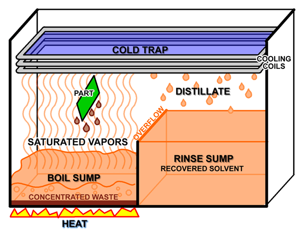
Gas phase cleaning, also known as vapor degreasing or, vapor phase cleaning is a procedure that boils a chemical solvent to produce steam, which then dissolves dirt and contaminants on the printed circuit board. Depending on the chemical solvent employed and the capacity of the solvents to be reused once contaminants are filtered, this process is regarded as effective and environmentally friendly.
The fluid is often designed based on the specific contaminants that must be removed, the temperature at which the chemical solvents boil, whether they are combustible or not, and whether they are environmentally friendly. The gas phase cleaning approach, like the ultrasonic method, is excellent for complicated PCBs because steam may reach small sections of a board that a physical brush may not be able to reach.
Deionized Water Wash
For eliminating water-soluble flux residue, deionized water is a safe and effective method. The method uses water-soluble flux in both leaded and lead-free pastes and solders, allowing them to be cleaned with deionized water. The in-line wash washes and rinses the PCB assemblies with deionized water jets at high temperatures and pressures. The water temperature is 144 degrees Fahrenheit, and the pressure is 45 pounds per square inch. After that, the assemblies are air dried using a series of driven air jets. To ensure cleanliness, resistivity, and ionics testing are utilized.
All PCBs produced by WORLD electronics are put through our Deionized wash.
Conclusion
A clean and clear PCB might also be advantageous during the inspection process or for future troubleshooting. When the board and all of its components are free of any remaining contaminates or leftover solder, it is much easier to locate faults or identify potential difficulties.
While choosing a PCB manufacturing partner think about cost optimization, adequate material usage, delivery time, and more. World electronics is your go to partner as we follow the latest IPC standards and tolerances and DFM and DFA rules to better suit your next upcoming PCB design.
To learn more about why we need to clean PCBs, refer to this article on our news page.
For more on WORLD’s capabilities, visit our services page and follow us on LinkedIn.
Related Articles
SMT, Thru Hole, Mixed Technology
Box Build/Higher Level Assembly